ULCOAT have produced prototype and mass production of glass MEMS to using of the processing technology of semiconductor mask blanks, large-sized mask blanks.
ULCOAT have produced prototype and mass production of glass MEMS to using of the processing technology of semiconductor mask blanks, large-sized mask blanks.
Micro devices such as μ−TAS、micro chemical systems, and DNA chips are formed on glass substrate with semiconductor technology.
MEMS(Micro Electro Mechanical Systems) also called micro machine or MST(Micro System Technology) are very useful devices, and the structures on the devices can be smaller than microns. Also they can be produced on silicon substrates and/or glass substrates using semiconductor technology.
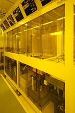
We offer all sorts of manufacturing process to carry out MEMS devices with glass substrate.
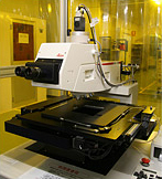
Double-sided Aligner
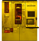
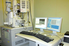
Electron-Beam Exposure System
Phoresist Delopment
CD Measurement
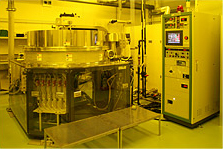
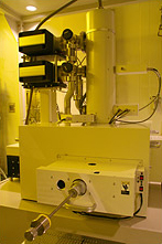
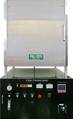
Sputtering
Wet etching bench
Borosilicate glass wet etch
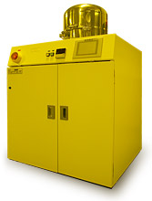
Blasting
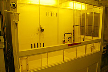
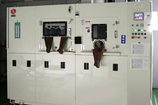
Oven for Glass direct Bonding
Direct bondings are possible to quartz glass, non-alkaline glass and borosilicate glass.
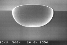
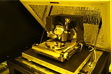
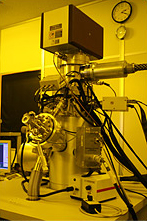
Scanning Electron Microscopy
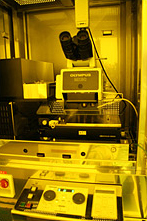
Atomic Force Microscopy
Auger Electron Spectroscopy
Micro-Raman Spectroscopy